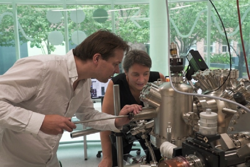
The pioneering single atom technology developed by the University of New South Wales (UNSW) scientists can be adapted to build 3D silicon quantum chips.
According to a recent report, the 3D architecture is considered a major step in the development of a blueprint to build a large-scale quantum computer.
Centre of Excellence for Quantum Computation and Communication Technology (CQC2T) researchers have shown for the first time that they can build atomic precision qubits in a 3D device.
They have demonstrated that they can extend their atomic qubit fabrication technique to multiple layers of a silicon crystal.
This helped them achieve a critical component of the 3D chip architecture that they introduced to the world in 2015.
Moreover, team members were able to align the different layers in their 3D device with nanometer precision.
This 3D device architecture is a significant advancement for atomic qubits in silicon.
To be able to constantly correct for errors in quantum calculations, one must be able to control many qubits in parallel.
The only way to do this is to use a 3D architecture. They, therefore, have developed and patented a vertical crisscross architecture in 2015.
However, there were still a series of challenges related to the fabrication of this multi-layered device.
With this current breakthrough, they have shown that engineering their approach in 3D is possible in the way they envisioned it a few years ago.
In this paper, the team has demonstrated how to build a second control plane or layer on top of the first layer of qubits.
They built the first plane, and then optimised a technique to grow the second layer without impacting the structures in first layer.
Since the surface of the second layer gets very rough, critics would say in the past, that what they did was not possible and that their precision technique can’t be used anymore.
Contrary to expectations, the team was able to do it.
Furthermore, the team members demonstrated that they can then align these multiple layers with nanometer precision.
If something is written on the first silicon layer and then a silicon layer is put on top, the location still needs to be identified in order to align components on both layers.
The team has shown a technique that can achieve alignment within under five nanometers, a feat considered as as quite extraordinary.
Lastly, the researchers were able to measure the qubit output of the 3D device single shot, which is using a single, accurate measurement, instead of relying on averaging out millions of experiments.
This research is a milestone in the field and they are working systematically towards a large-scale architecture that will lead to the eventual commercialisation of the technology.
While they are still at least a decade away from a large-scale quantum computer, the work of CQC2T remains at the forefront of innovation in this space.
Concrete results such as these reaffirm their strong position internationally.


